You are using an out of date browser. It may not display this or other websites correctly.
You should upgrade or use an alternative browser.
You should upgrade or use an alternative browser.
Toshiba USB to SATA Guide
- Thread starter Jared
- Start date
michael chiklis
Member
I don't think they're too short, problem could be elsowhere.
Can you show us your soldering job with a pic?
Can you show us your soldering job with a pic?
michael chiklis
Member
Yes, they're too long wires.
When i soldered wires to convert usb to sata, they were much more short but drive was still very unstable.
When i soldered wires to convert usb to sata, they were much more short but drive was still very unstable.
SilverPuppy
New member
michael chiklis":3fk4z721 said:Unfortunately there isn't a way to write rom on donor sata pcb via serial mode, but i'll explain you how to write it without taking off chip from donor pcb by using eprom programmer.
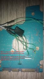
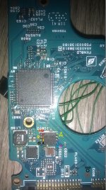
This task is hard, you'll need good soldering skills with classic soldering iron, steady hand, good magnifying glass and time, but at least you can do it without unsoldering rom chip from sata pcb.
Need to solder 6 thin wires, or just 5 wires due to fact that it will not be necessary to apply on rom Vcc power with your eprom programmer, just power on sata pcb by using computer sata cables to easily supply Vcc on rom chip.
View attachment 4View attachment 3View attachment 2View attachment 1
Vcc is ROM pin 8, pin 3 and 7 are natively jointed together on board to pin 8.
This means that pins 3 - 7 - 8 are in common.
You're a hero. You didn't specify where to put the vcc wire though, so I'll have to figure it out. (Although if 3, 7, and 8 are joined at the board why would that be needed?) Water-damaged board won't power up. I'm hoping to read the water-damaged one this way and maybe even write it to the new board this way, as with my current toolset that would probably be easier (and definitely be safer) than removing the chip.
Any reason a CH341A based programmer couldn't handle this task?
michael chiklis
Member
SilverPuppy":3s4kpdvy said:[post]8958[/post] You're a hero. You didn't specify where to put the vcc wire though, so I'll have to figure it out. (Although if 3, 7, and 8 are joined at the board why would that be needed?)
Have you read carefully my post?
posting.php?mode=edit&f=29&p=8871
Have you seen carefully my pics?


If you know the basics of electronics, you should know that you can choose where to solder the Vcc wire (pin 8 or pin 7 or pin 3).
I choosed to solder wire on pin 3 (there is a reason why i've coloured pin 3 - 7 - 8 in yellow colour).
Regarding Vcc line (yellow points), you neither need any of those if you use usb power supply.
Of course, reading/writing rom on board will work only if there isn't any short circuit on Vcc power line, if your pcb has short circuit you should consider to physically transfer rom (seek a pro).
You should first check ROM datasheet to insure at what voltage does it work.SilverPuppy":3s4kpdvy said:[post]8958[/post] Any reason a CH341A based programmer couldn't handle this task?
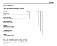
Typical rom that you can find on these toshiba pcb is 25P40V6 which needs power supply between 2.7V - 3.6V

then find out if your eprom programmer provides proper power supply to rom, if is higher (example 5V) then definitely you shouldn't use on your rom because it can kill it.
Besides power supply, you eprom should support SPI 25 series roms
SilverPuppy
New member
Thanks for the help everyone. Sorry for appearing to have not paid attention to your diagrams and such; I was a little confused, basically because I've been sick and apparently forgotten how to count. :roll: My boards are USB and as such some of the solder points are in a little different place than they are on your SATA board, but they're pretty obvious because the traces are clearly visible.
I don't have access to an ultrasonic cleaner at the moment, but agree that it would be an excellent strategy if I did. I'm going to see if I can clone the ROM from the old to the new without removing them from the board. I will post the result for sure.
I don't have access to an ultrasonic cleaner at the moment, but agree that it would be an excellent strategy if I did. I'm going to see if I can clone the ROM from the old to the new without removing them from the board. I will post the result for sure.
michael chiklis
Member
Remember, use only your usb power supply, if that doesn't work then give power to rom by using eprom programmer.
Do not use both together!
Do not use both together!

